retrofox
Newbie

Joined: May 2019
Posts: 5
Location:
|
Post by retrofox on May 1, 2019 21:41:43 GMT
Hi there. Im trying to mod a VA0.5 NTSC-J Saturn with Sebs switchless mod. When switching to 50hz the screen goes black with some glitchy lines allover the screen. I read that I needed to lift pin 79 of IC14 since the JP1&2 jumpers are also connected to the clock. After following traces I come up with this idea but no success. I assumed the second trace from the jumpers went to the clock Red= cut traces. Blue = Wires. 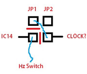 Have I made a mistake where the clock trace is? Is there a way I can do this without messing with pin79 as Im worried I may snap it or accidentally bridge the the other pins with solder. Am I correct thinking the trace I labeled is the clock? or did I get this wrong? Thanks for reading. |
|
retrofox
Newbie
Joined: May 2019
Posts: 5
Location:
|
Post by retrofox on May 2, 2019 13:30:26 GMT
Oh id also like to note its not the cable, I have 5 modded NTSC-J model 2's with no such issue on the same cable.
|
|
|
|
Post by zyrobs on May 2, 2019 19:33:16 GMT
VDP2 pin 79, PLL pin 1 (I think), and the pal/ntsc encoding selection pin on the video encoder (forgot which one), are all connected together. The JP1 and JP2 jumpers just select whether to connect this common trace to +5V or GND. Lifting the VDP2 pin is recommended because then you don't have to worry about any of the other traces (depending on Saturn version, there may be less or more stuff on that line).
The PLL pin 1 controls a clock speed selection divider, so PAL units can still get the 28.6MHz clock despite using different main clocks. This main clock is also tied to the dot clock of the video output, so you'll end up with a rolling image. And the console possibly crashing due to half the system running at the wrong speed.
From your description, it sounds like you cut a wrong trace. Do a continuity test between the VDP2 pin and the PLL pin. On a NTSC units, I think that PLL pin should be +5V. Keep in mind, that many of the traces run under the chips, so it's possible that there was something there you did not see.
|
|
retrofox
Newbie
Joined: May 2019
Posts: 5
Location:
|
Post by retrofox on May 2, 2019 20:11:01 GMT
Ah so im guessing my only option is to lift pin 79 to solve this? Wile restoring JP1/2 back to normal.
|
|
|
|
Post by zyrobs on May 2, 2019 20:12:07 GMT
Nevermind, I looked at the board, I see what your pic is supposed to be now: 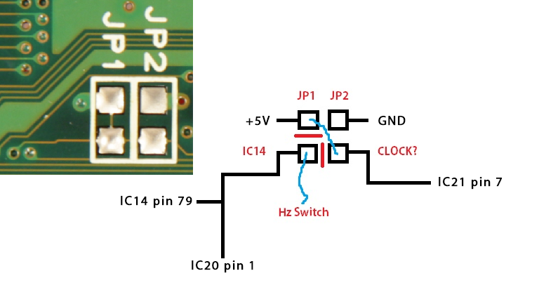 The trace connecting VDP2 pin 79 and PLL pin 1 is under the VDP2, so you did not see it. That's why most guides recommend lifting the VDP2 pin, because then you don't have to worry about the PLL connection, which is at a different place on every board. Fastest fix would be to cut the trace between the VDP2 and PLL, and wire the PLL separately to +5V. I think one of the three vertical vias near the closest CD Drive support peg hold closest to the PLL area should be one of them, you'll have to trace it. Cut it on the underside of the board, then run a 24 or 28AWG single strand wire through the other via that leads directly to PLL pin 1 on the top, and connect it to the positive side of any of the nearby caps. Also note, soldering through the board vias is simpler and safer than lifting pins. Of course, you still need to know the correct traces to cut and solder to, whereas with pin lifting, the entire point is that you disconnect the pin from the rest of the system, so you don't have to worry about that. OR, you can just not bother adding 50/60 mods to NTSC units, since it really is quite pointless, and both harder to do and less compatible than modding a PAL unit to 60Hz. |
|
retrofox
Newbie
Joined: May 2019
Posts: 5
Location:
|
Post by retrofox on Jun 4, 2019 1:24:10 GMT
Im late to return so now the pictures ent' loading but figured it from your words thankfully =D
Going to leave some extra info here for other people who may need it.
PLL is IC20.(top of board, between drive mount legs)
Pin 1 needs to be attached to 5v. The 5v is on the JP1 jumper (the side right to the JP1 text)
Cut traces (or remove jumpers) joining to the other side.
My method to do this was to slide a hair through the closest via to IC20 pin 1 (very close) Then I can see where it shows on the other side, I then cut the trace after the via on the back side of the board.
I then solder the via(backside of board) to the 5v on jp1. (this way the wire doesn't need to wrap around the board)
I can now attach my 50/60hz switchless mod wire directly to the regular area shown in most guides.
This does seem like the safest method possible with no chance of damaging chips, the little exta work is worth it.
Edit: tested and worked perfectly, thanks for the help =)
|
|


